Sign In | Join Free | My himfr.com
Home > ALTERA FPGA Chip >

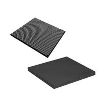
EP2AGZ300FF35I4N 554 I/O 11920 LABs ALTERA FPGA Chip

    Buy cheap EP2AGZ300FF35I4N 554 I/O 11920 LABs ALTERA FPGA Chip from wholesalers
     
    Buy cheap EP2AGZ300FF35I4N 554 I/O 11920 LABs ALTERA FPGA Chip from wholesalers
    • Buy cheap EP2AGZ300FF35I4N 554 I/O 11920 LABs ALTERA FPGA Chip from wholesalers

    EP2AGZ300FF35I4N 554 I/O 11920 LABs ALTERA FPGA Chip

    Ask Lasest Price
    Brand Name : Intel / Altera
    Model Number : EP2AGZ300FF35I4N
    Certification : Lead free / RoHS Compliant
    Price : USD 4000-5500 pcs
    Payment Terms : T/T, Western Union, Paypal, Trade Assurance, Credit Card
    Supply Ability : 126 pcs
    Delivery Time : 3-5 Day
    • Product Details
    • Company Profile

    EP2AGZ300FF35I4N 554 I/O 11920 LABs ALTERA FPGA Chip

    EP2AGZ300FF35I4N ALTERA FPGA Chip FBGA-1152 554 I/O Arria II GZ


    Product AttributeAttribute Value
    Intel
    FPGA - Field Programmable Gate Array
    Arria II GZ
    298000
    11920
    554 I/O
    1.5 V to 3.3 V
    - 40 C
    + 85 C
    SMD/SMT
    FBGA-1152
    Tray
    Data Rate:600 Mb/s to 6.375 Gb/s
    Series:Arria II GZ
    Brand:Intel / Altera
    Embedded Block RAM - EBR:3725 kbit
    Maximum Operating Frequency:540 MHz
    Moisture Sensitive:Yes
    Number of Transceivers:16/24 Transceiver
    Product Type:FPGA - Field Programmable Gate Array
    Factory Pack Quantity:24
    Subcategory:Programmable Logic ICs
    Total Memory:18413 kbit
    Tradename:Arria
    Part # Aliases:971029

    Arria II GX devices have dedicated configuration banks at Bank 3C and 8C, which support dedicated configuration pins and some of the dual-purpose pins with a
    configuration scheme at 1.8, 2.5, 3.0, and 3.3 V. For Arria II GZ devices, the dedicated configuration pins are located in Bank 1A and Bank 1C. However, these
    banks are not dedicated configuration banks; therefore, user I/O pins are available in Bank 1A and Bank 1C.

    Dedicated VCCIO, VREF, and VCCPD pin per I/O bank to allow voltage-referenced I/O standards. Each I/O bank can operate at independent VCCIO, VREF, and
    VCCPD levels.

    Auto-Calibrating External Memory Interfaces
    ■ I/O structure enhanced to provide flexible and cost-effective support for different types of memory interfaces
    ■ Contains features such as OCT and DQ/DQS pin groupings to enable rapid and robust implementation of different memory standards
    ■ An auto-calibrating megafunction is available in the Quartus II software for DDR SDRAM, DDR2 SDRAM, DDR3 SDRAM, RLDRAM II memory interface
    PHYs; the megafunction takes advantage of the PLL dynamic reconfiguration feature to calibrate based on the changes of process, voltage, and temperature (PVT).

    Quality EP2AGZ300FF35I4N 554 I/O 11920 LABs ALTERA FPGA Chip for sale
    Inquiry Cart 0
    Send your message to this supplier
     
    *From:
    *To: CHUANGXINDA ELECTRONICS-TECH CO., LIMITED
    *Subject:
    *Message:
    Characters Remaining: (0/3000)