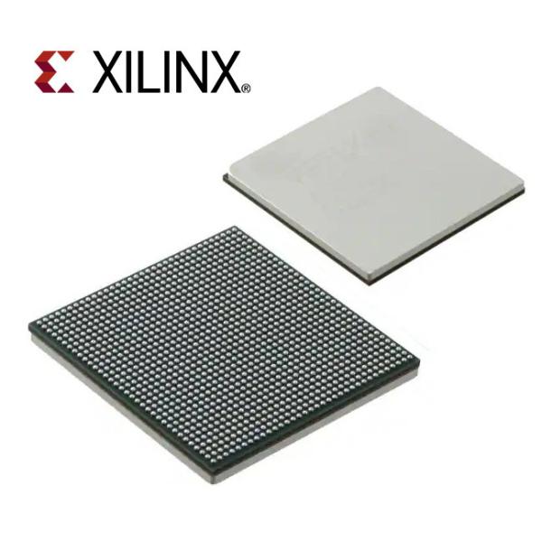
Take Innovation to the Next Level with Highest-Capacity FPGAs
• SSI technology delivers 2 million logic cells, 85Mb block RAM,
and 3,600 DSP48E1 slices for new possibilities of integration and
performance
• 28nm high- metal gate (HKMG) HPL process reduces core power by
50%
• 0.9V core voltage option for even lower power Choose Between
Three Varieties of Low-Power Serial Transceivers
• 12.5 Gb/s GTX transceivers for broad support of mainstream serial
protocols
• 13.1 Gb/s GTH transceivers support the 25% overhead for FEC
standards for proprietary interfaces and full 10GBASE-KR compliance
• 28.05 Gb/s GTZ transceivers support next-generation optics
• Obtain assured compliance with popular standards such as
10/40/100G Ethernet, PCI Express®, OC-48, XAUI, SRIO, and HD-SDI
Achieve Your Performance Targets Easily
• Gain a 2x performance improvement: the parallelism of the FPGA
architecture enables more work with each clock cycle to deliver
higher performance with lower power
– Up to 56 12.5 Gb/s transceivers
– Up to 96 13.1 Gb/s transceivers
– Up to 16 28 Gb/s transceivers
– Up to 2 million logic cell capacity enabled by SSI technology
– Up to 85Mb block RAM for high-bandwidth data buffering
– Up to 5.3TMACS signal processing performance enabled by 3,600
DSP48E1 slices
• Implement 1.6 Gb/s LVDS interfaces with enhanced SelectIO™
technology that reduces I/O power by up to 50%
• Build up to eight 72-bit interfaces for DDR3 memory (up to 1,866
Mbps)
• Interface to legacy devices with 3.3V-capable I/O
• Meet the most stringent timing requirements with powerful clock
management tiles (CMTs) that combine a phase-locked loop (PLL) and
a mixed-mode clock manager (MMCM) for high precision and low jitter
clocking Bring Your Product to Market Faster
• Achieve maximum FPGA performance with ISE® Design Suite 13
• Design faster and reduce risk with pre-verified IP cores
• Debug logic and serial interfaces quickly with the real-time
verification capabilities of ChipScope™ Pro tools
• Vivado™ Design Suite


